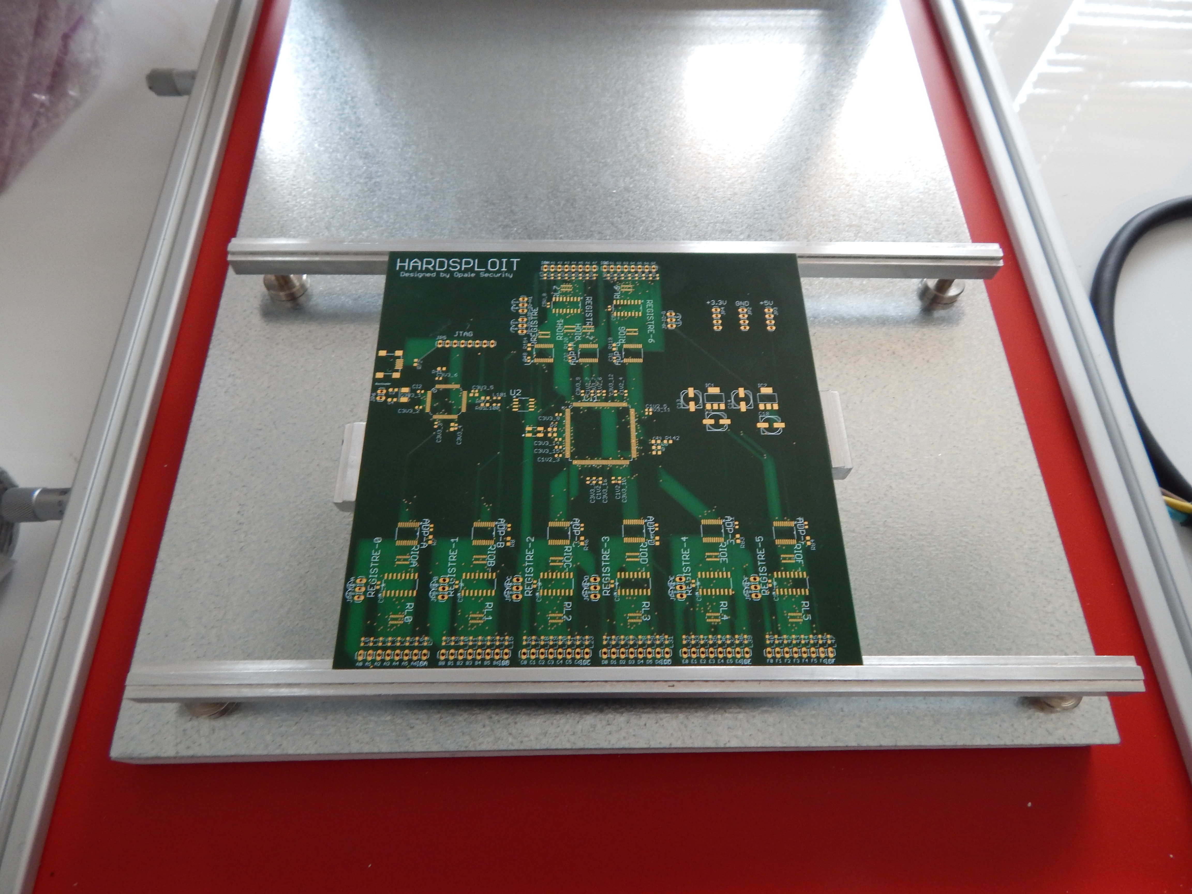
We have made some change and improvement to reduce the size of the electronic board
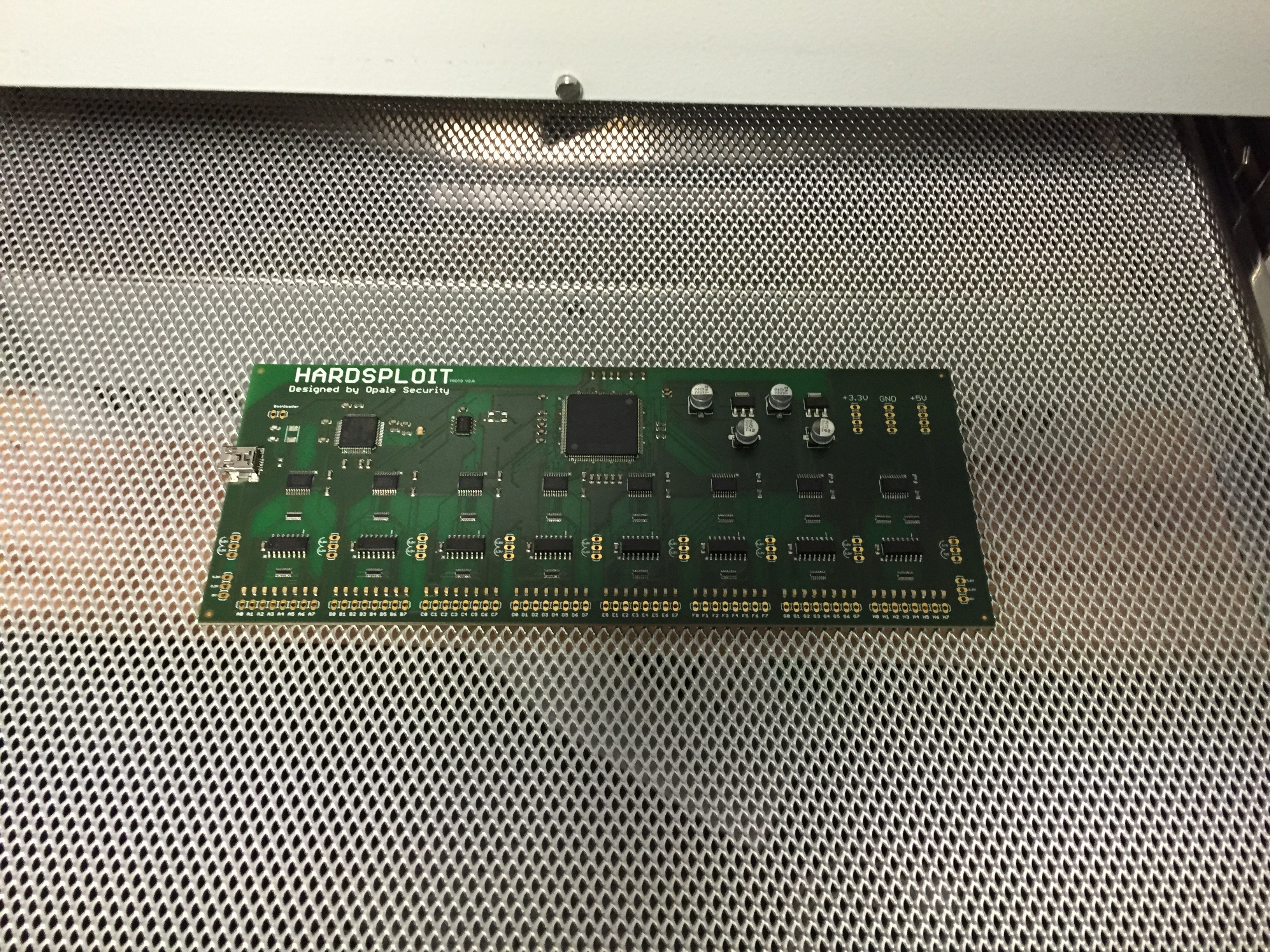

We have made some change and improvement to reduce the size of the electronic board
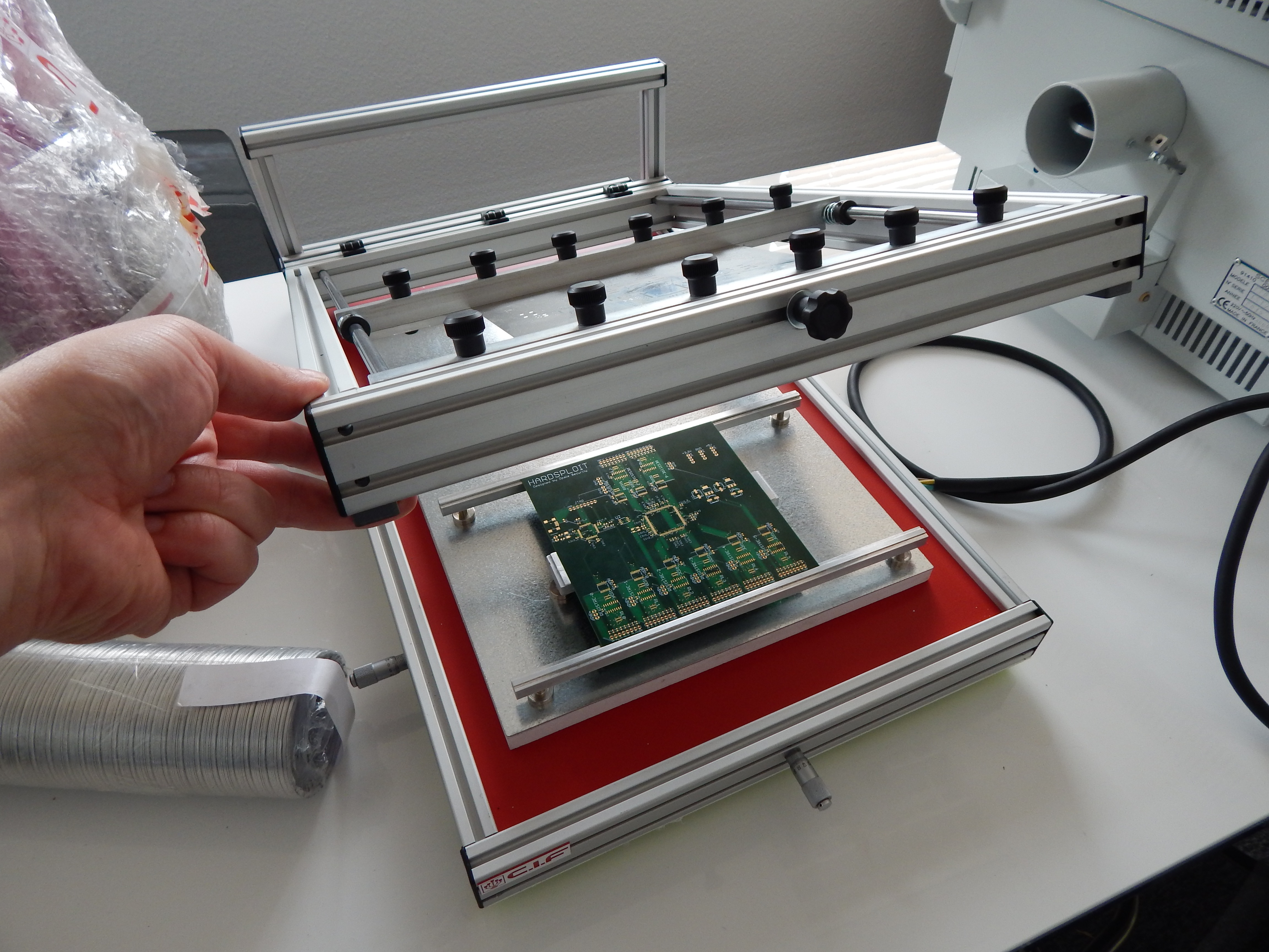
Thanks to our financial Partners (Region Bretagne @regionbretagne, @BretagneBDI , @lameito…), we succeed to update our electronic production line.
The goal is to be able to produce small series @ Opale Security Lab in a more effective way
As explain on Adafruit Web site,
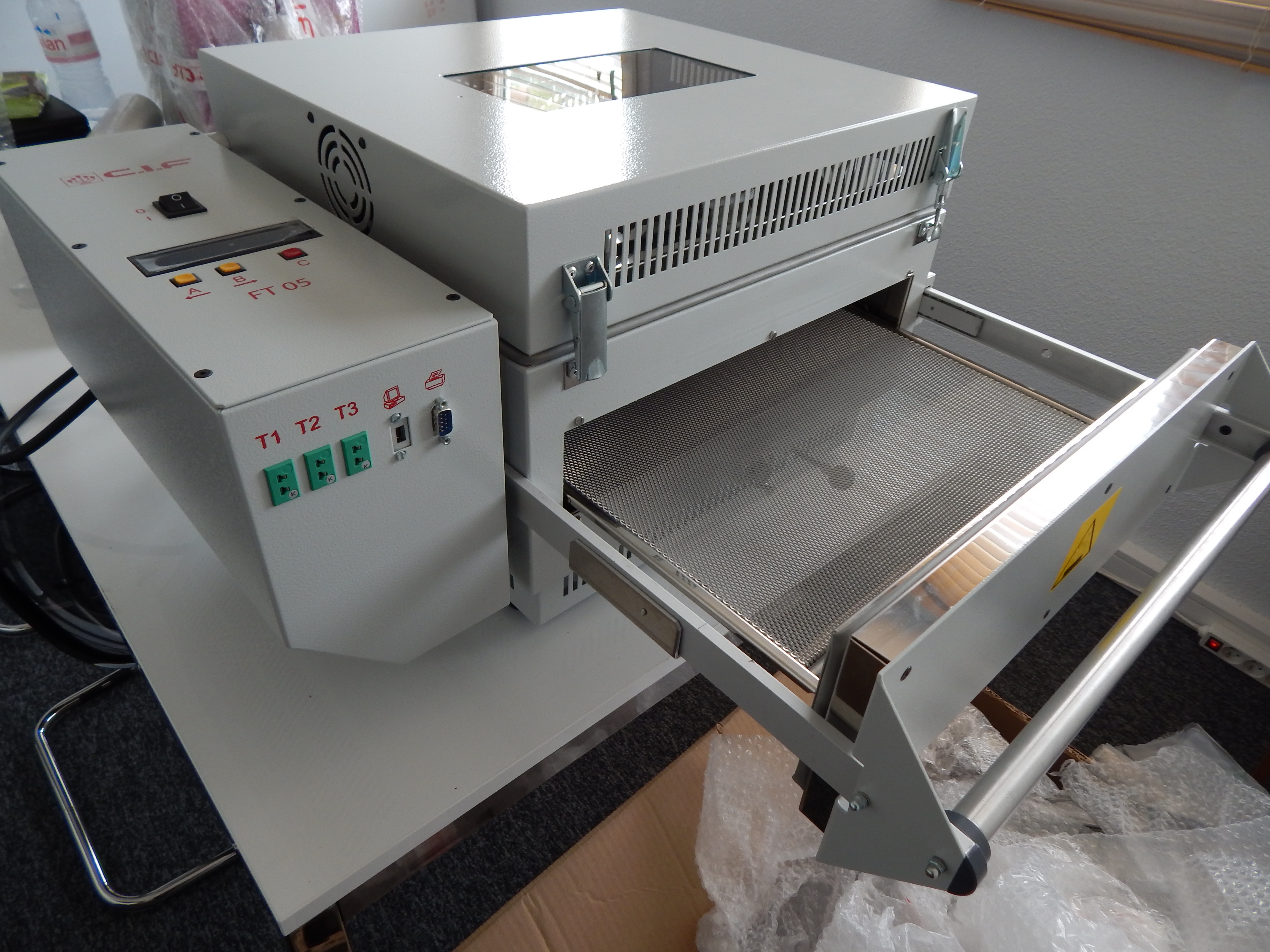
Stencil machines hold the metal-cut stencil flat and taut so that you dont have any shifting or curling while you try to lay paste down. The good ones have a fixture so you can always get the same alignement every time – speeding up your stenciling time down to under a minute per PCB
We choose A C.I.F machine. See below
As the Hardsploit Core Framework is over, we continue with the development of Hardsploit modules. A Hardsploit Module is like an Exploit Module for Metasploit. It’s a piece of FPGA code that have a dedicated hacking (or auditing ;-)) function; Each module will offer functionalities such as dump, read & write, interact, Proxy or sniff etc.
To begin, we have designed a module related to parallel memory. Why? Mainly because, to our knowledge, there is no tool that can achieve that in a simple way.
Summary of Hardsploit Internal Communication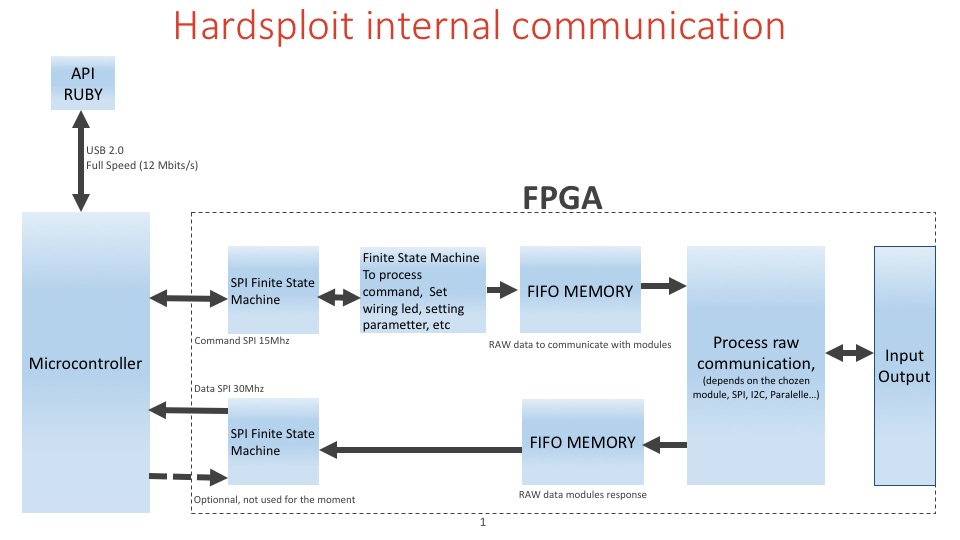
The parallel memory module for example, looks like the following. It will use the Core FPGA Hardsploit module.
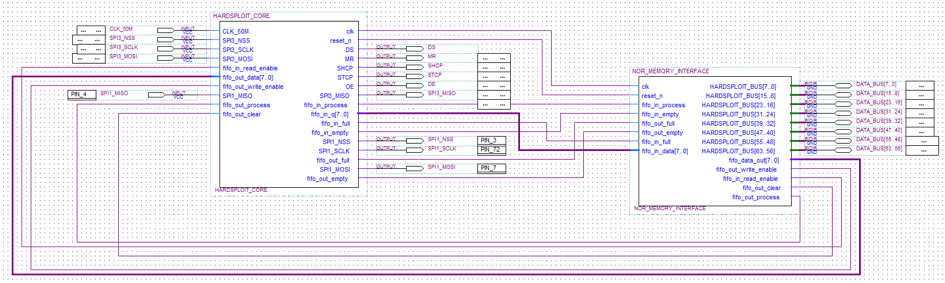
Harsploit core module is a bit complicated stuff
Simple? 🙂 Maybe a flowchart could help (or not ?)
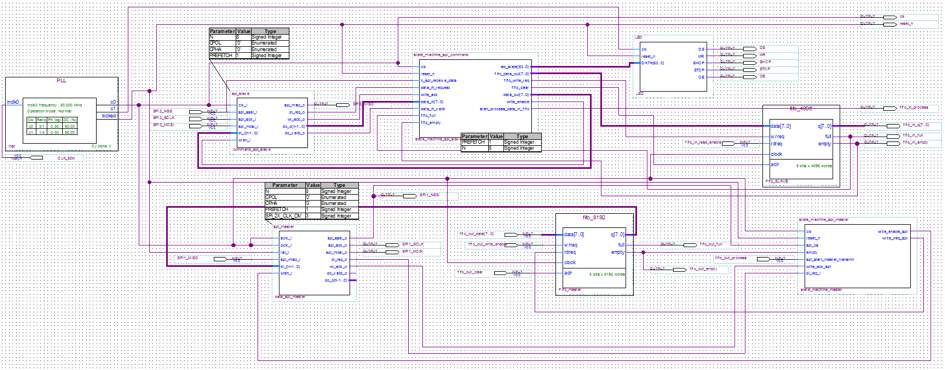
In brief, we have created a FPGA module that is able to dump most of parallel memory chip. It will help security pentesters to dump firmware or all content contained in such memory in a easy way.
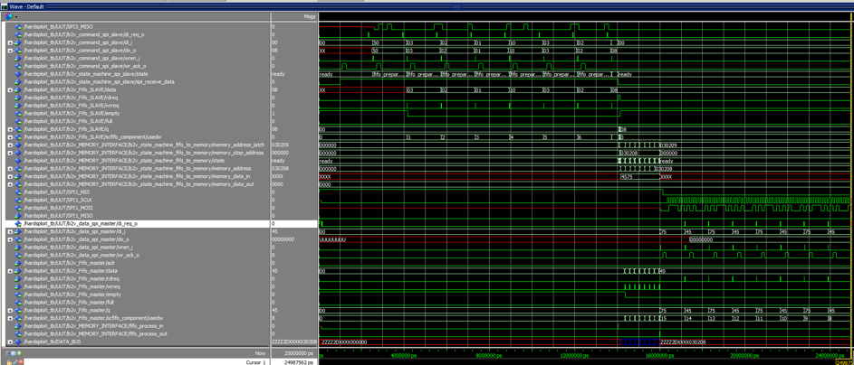
During our simulation and testing step, we succeed to dump parallel memory command with 3x8bits for address (see Graph Below)
What type of Memories we could dump for now?
Performance? Dumping Speed achieved (real world example – no bullshit)
For example, a dump of 128MByte memory chip.
More on dumping performance, according to our test ,
Just try to achieve that with other existing solution 😉
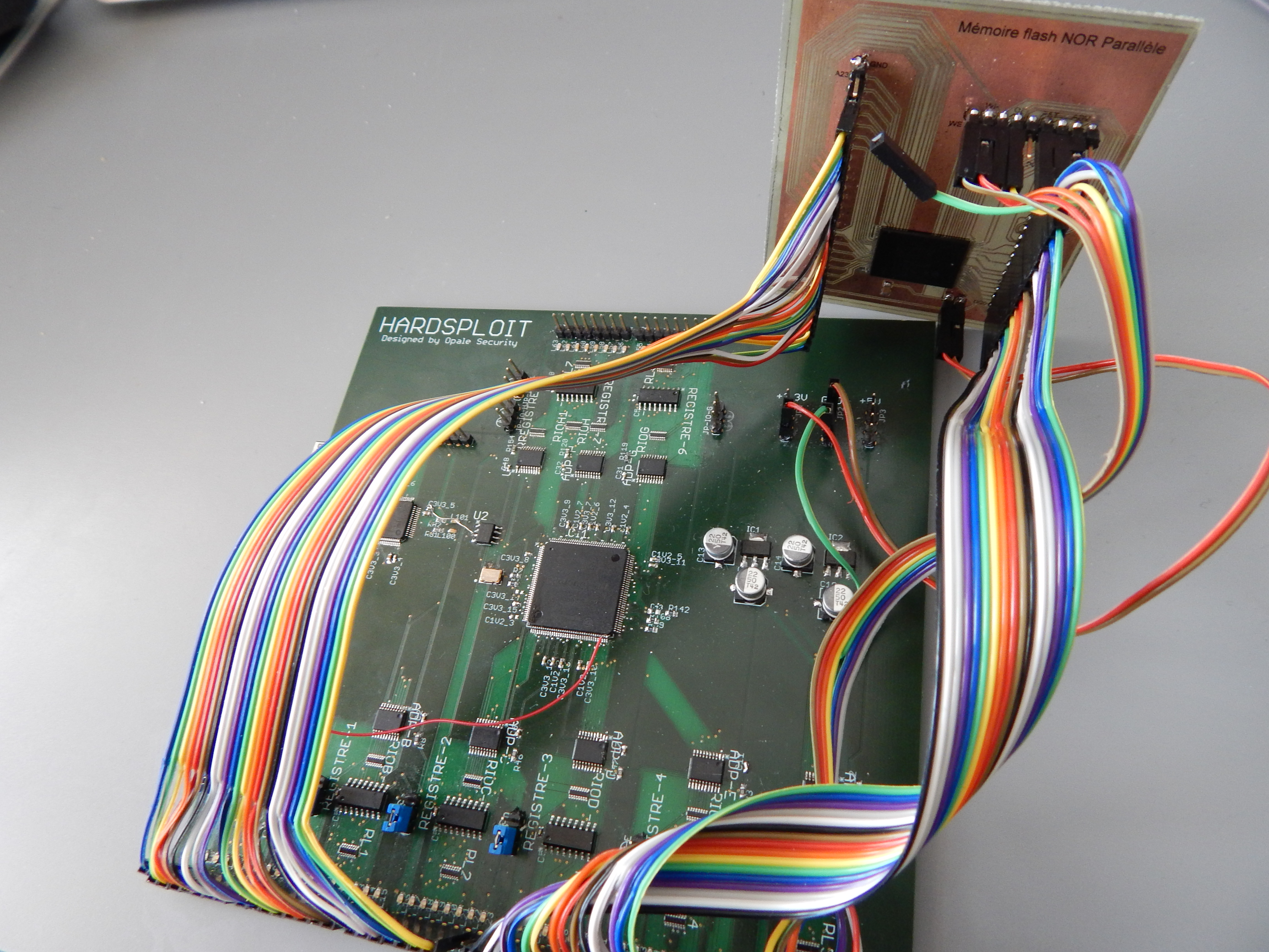
How to use that funky and (over) hype parallel dumping and writing function ?
We use our API (soon linked with the GUI…stay tuned)
We create a low level API with ruby that let you interact with FGPA module (Harsploit Module) in a simply way. See below an example of code we use. One function to call , few parameters to send (block to dump), few command to drive the chip. All those parameters will be soon pre input via the use of the GUI.
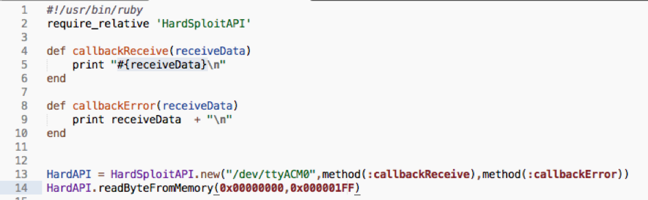 Simple as that !
Results (with testing values – interesting data is at the beginning of the block)
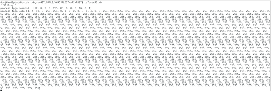
Now you need to reverse the content of this memory and it’s your pentesters’ job 🙂
More information coming soon about several other Hardsploit Modules (I2C, SPI etc…)
As an image could help to understand how “things” work. Please find below a graphic that shows most of HardSploit Internal communications.

Because all is not always about PCB, soldering and blinking leds, here is a post with more information about our technological choices concerning the way Harsploit will communicate with higher level layers. You will notice that some choices we’ve made are not necessarily dicted by a given technology but in contrary because it’s seemed fun , useful and interesting to achieve our functional goals : create an easy to use Hardware Hacking Framework !
Here is a graphic summary for those who are in a hurry :

The concept behind Hardsploit when the idea came up was “Make the hardware pentesting more accessible and more flexible”. What we mean by that ? Well, in few clicks you must be able to get the content or hack the electronic components you’re working on. So yes, if it wasn’t already clear in your mind there is a graphical interface, but don’t worry if you are more a command line person we haven’t forgotten you.
Why Ruby in particular ? First thing is, we were interrested to know more about it and then because we realize that it is very “smooth” to use (the gem system is very convenient, the simple syntax even more). No technical reasons here, we are not limited by it, technically speaking, and we hope that will continue this way (apparently no reason the inverse happen).
Is it still necessary to introduce it ? Logic choice for local/client storage, work great with Ruby and perfect system interoperability.
No doubt one of the most useful thing we use with Ruby. Define the database model, forget raw SQL. An invaluable time saving. As a security company that perform application pentesting we are still curious to know how it handle SQLi attempts…
We aren’t using it with Rails, just the activerecord core.
Finally the graphic part: We are using the well knowed Qt library (which is compatible with the most common platforms, a strong asset) to create the Hardsploit interface. Using Qt and the Qt designer with Ruby requires some tweak that are explain below:
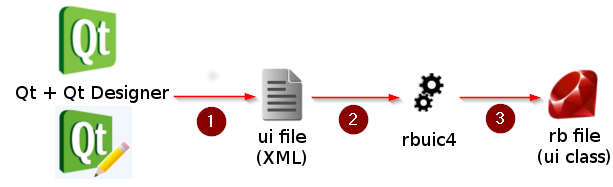 Step 1 -> Create the visual with Qt Designer, get a .ui file
Step 2 -> Use rbuic to convert the ui file to Ruby:
file.ui -o file.rb
Simple as that !
Our CrowdFunding Campaign for HardSploit project is started.
https://www.indiegogo.com/projects/hardsploit-like-metasploit-but-for-hardware
We will appreciated your help 😉

After few weeks of Works, we may say that the Hardsploit Hardware prototype is validated !
Only one wire errors 😉 see screenshot below
Simple FPGA Module update function via USB is OK. Even if Bit flipping may add some stress when you debug such sort of updating process 😉 !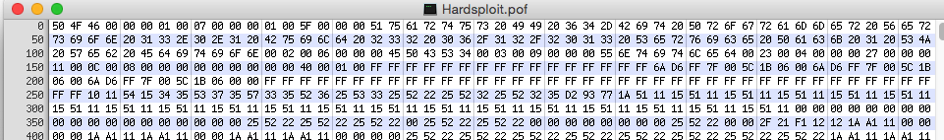
Now, if users want to scan an I2C bus, they just need to :
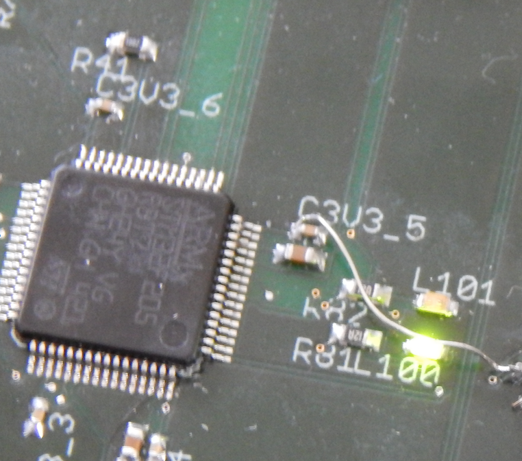
And of course Leds are working great : Visual Helping Wiring function is in development (In progress)
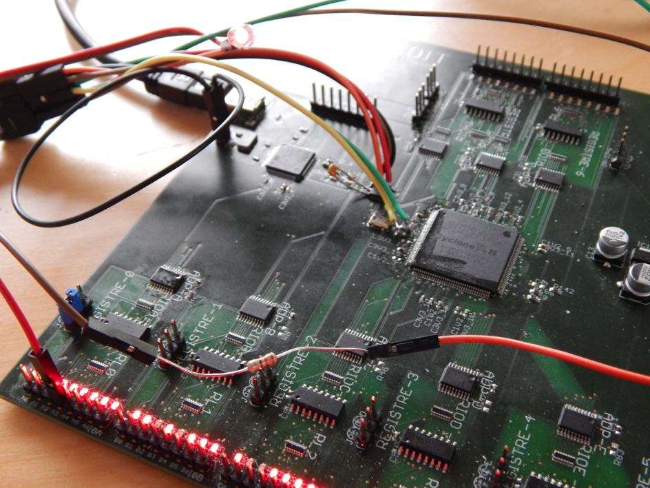
The HardSploit Team is ready for VHDL module development and test
Stay tuned
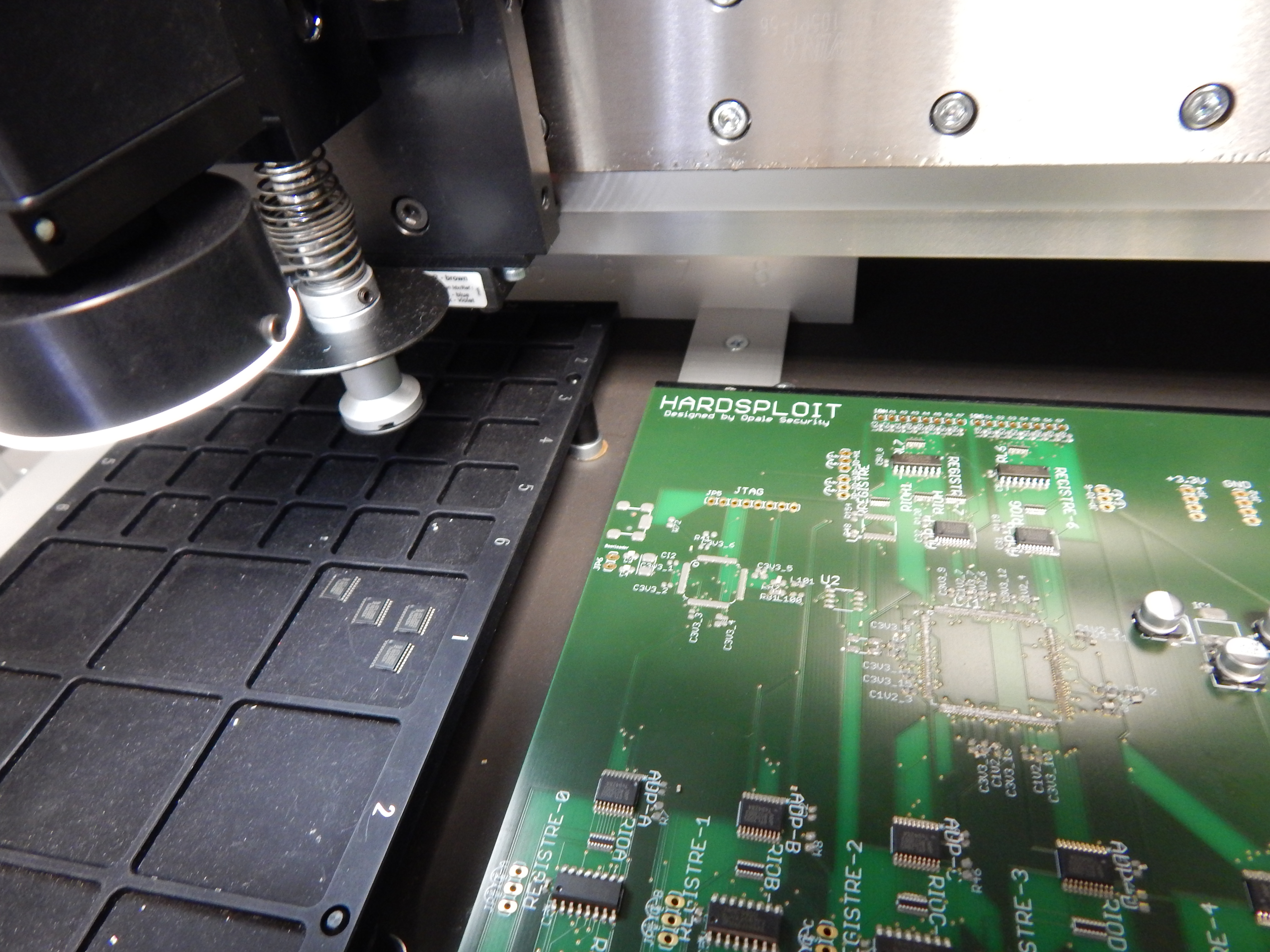
All components are now on our PCB prototype. We need to solder all Pins. Reflow soldering is the most common method for attaching surface components to a circuit board.
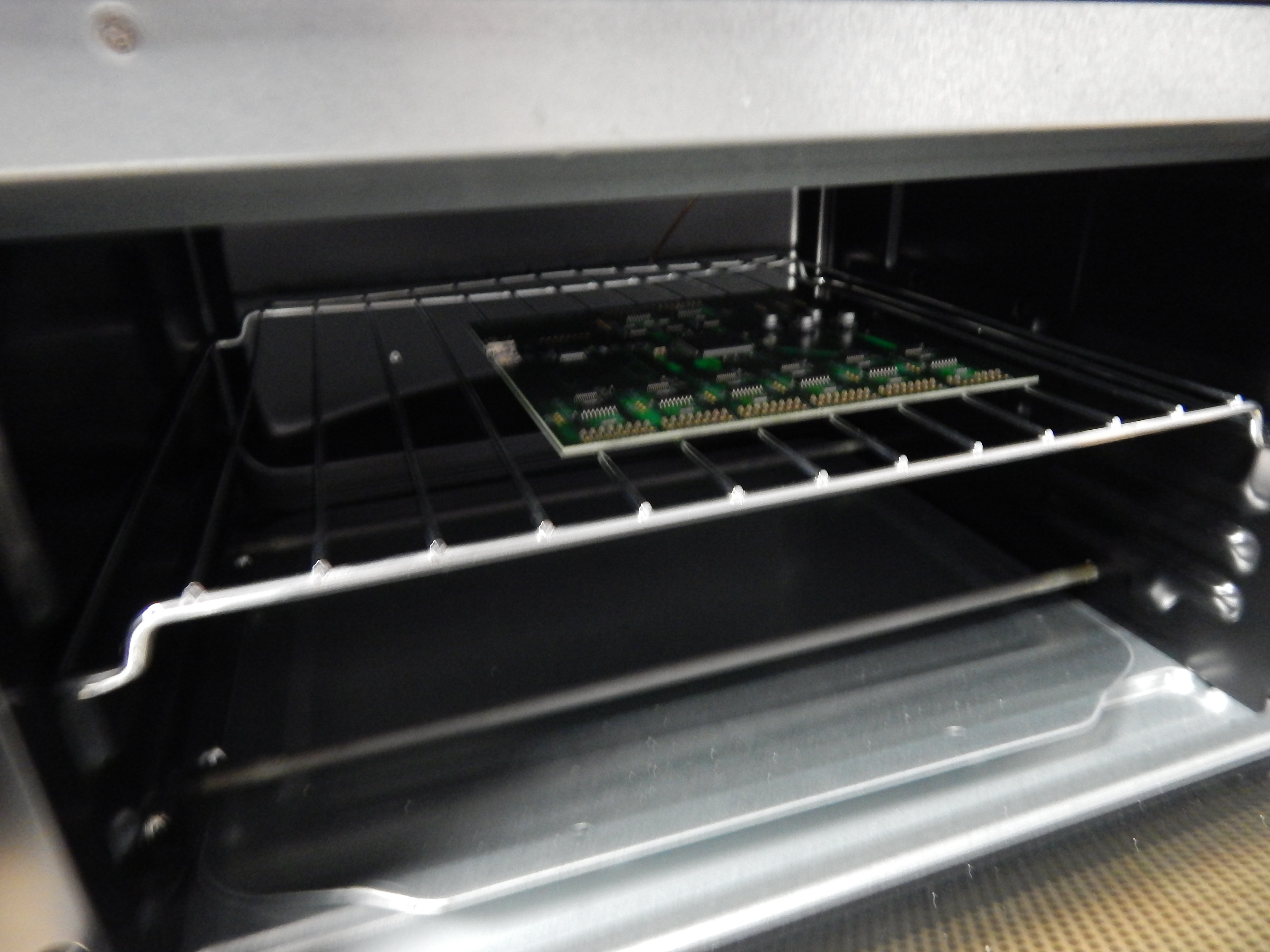

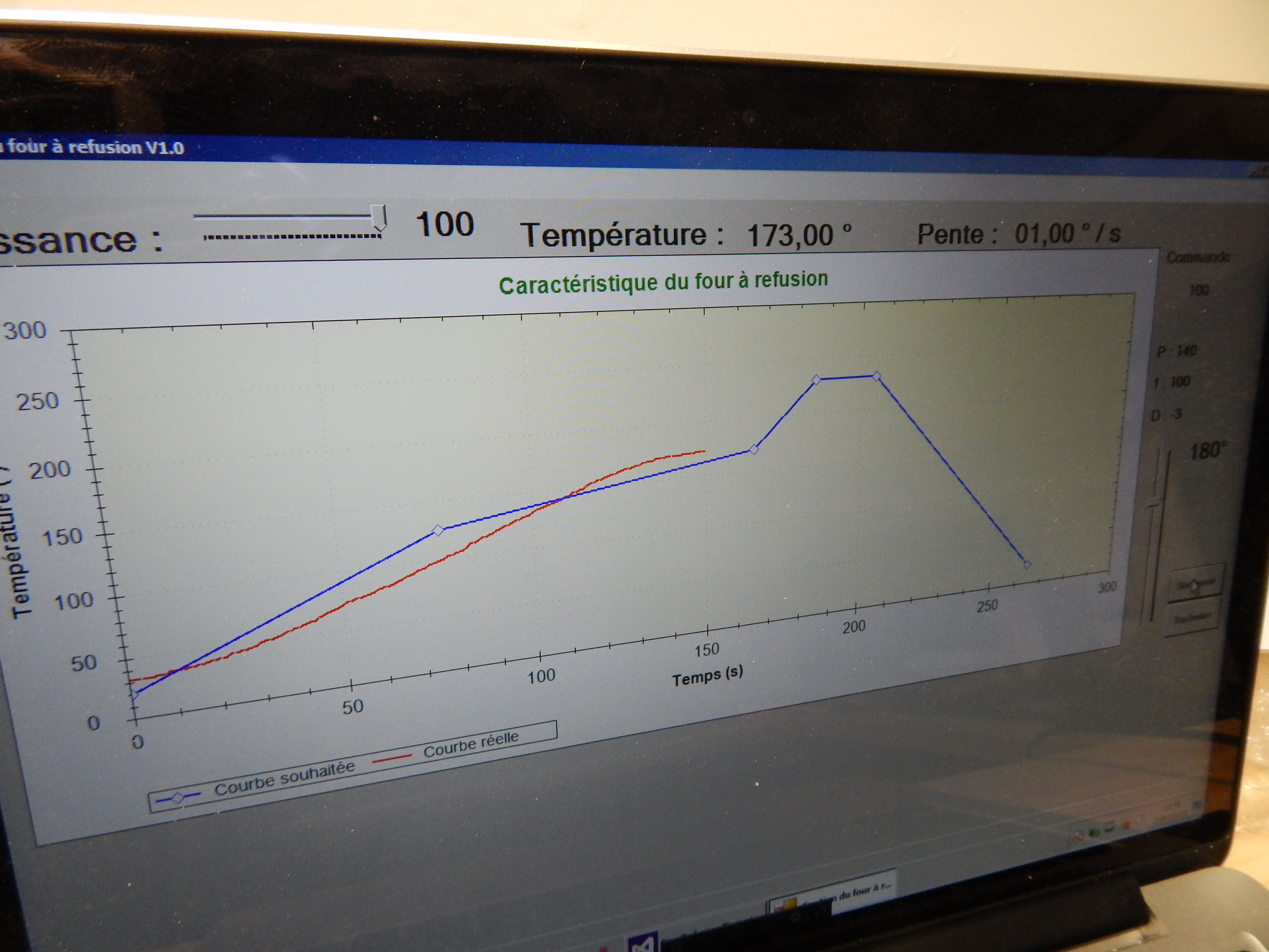
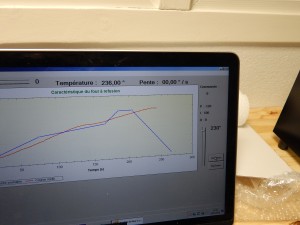
After dispensing the solder past (cf last post), we begin to use the pick & place machine to put all SMT components automatically on PCB Board.
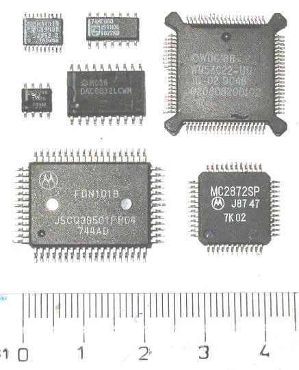
First, just remind that SMT components are (very!) small parts :


Even powerful integrated circuits are small parts : FGPA, MicroController,etc. :
After having perform all setups of the pick & place machine, we have to feed it with several tapes of SMT components:
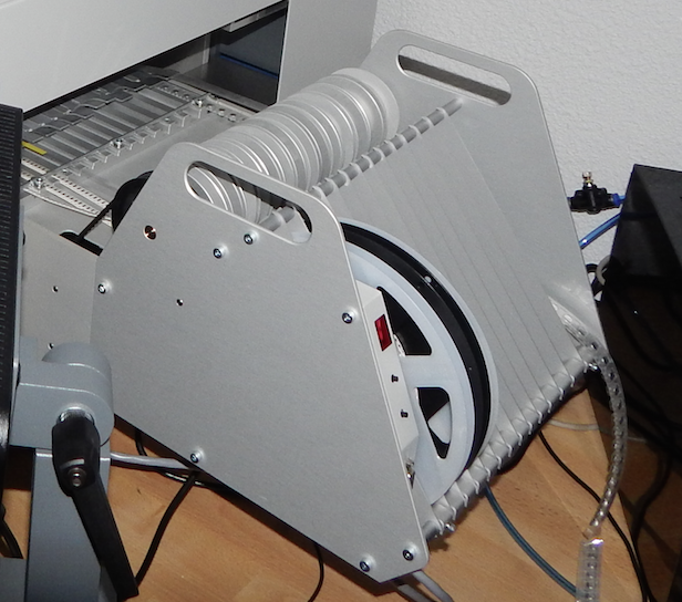
And we installed all those tape on the Feeders of the pick&place machine
Pick & Place is ready to start
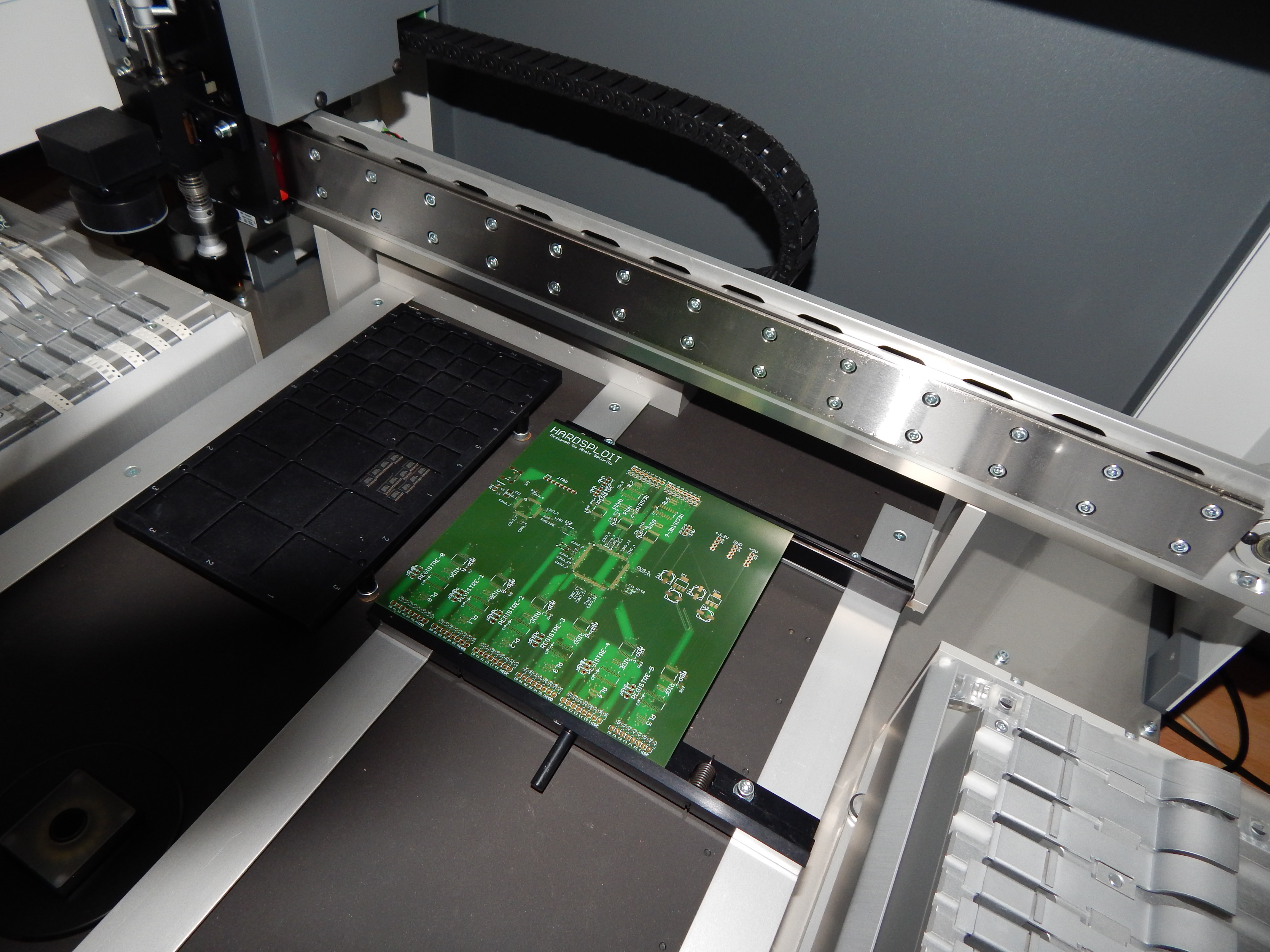
And here are the beauty of pick & place process 🙂 less than 7 mn to wait (but we cut the video for you)
Final result : all electronics component are in place on the PCB board