
As the Hardsploit Core Framework is over, we continue with the development of Hardsploit modules. A Hardsploit Module is like an Exploit Module for Metasploit. It’s a piece of FPGA code that have a dedicated hacking (or auditing ;-)) function; Each module will offer functionalities such as dump, read & write, interact, Proxy or sniff etc.
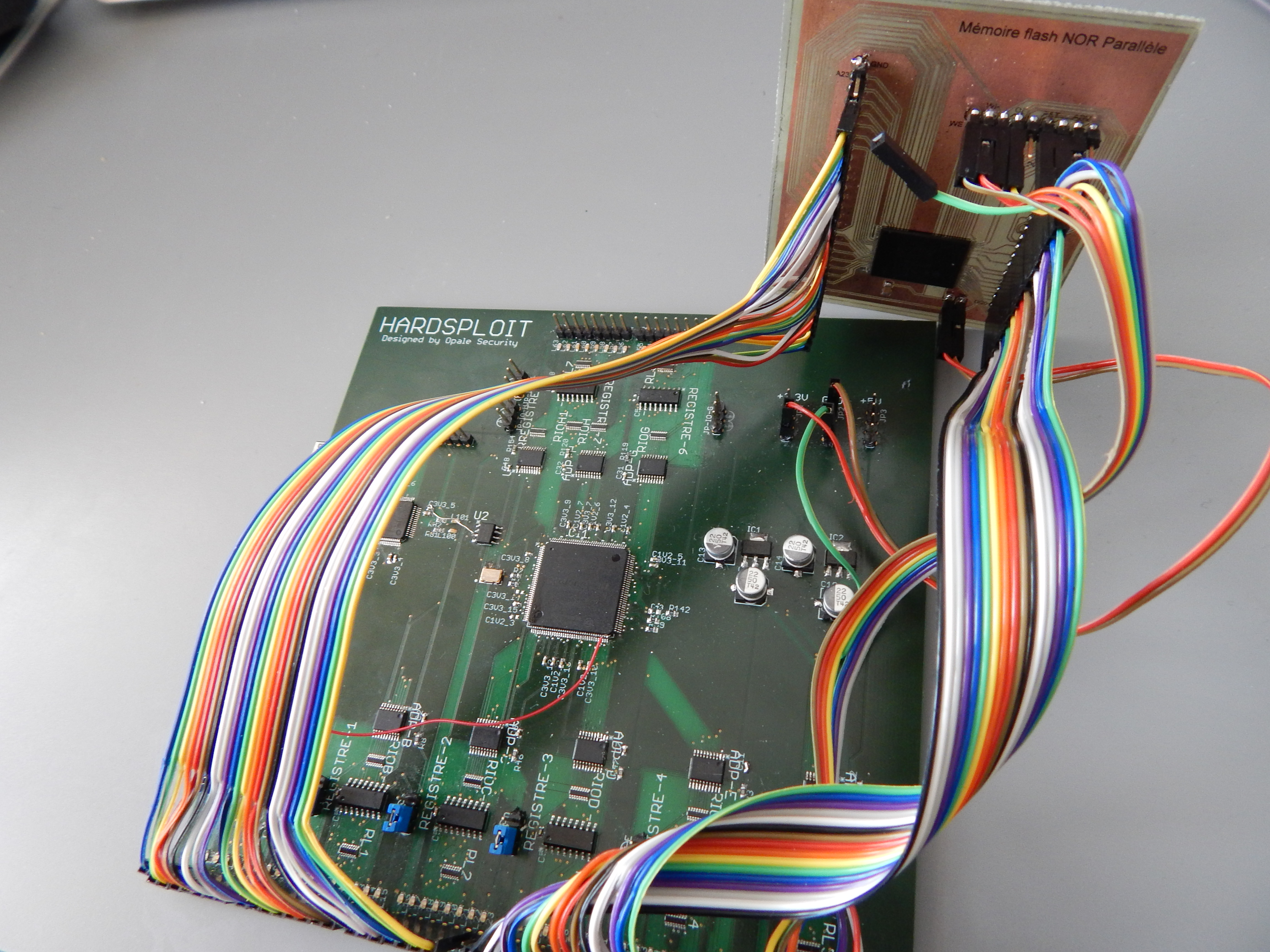
To begin, we have designed a module related to parallel memory. Why? Mainly because, to our knowledge, there is no tool that can achieve that in a simple way.
Summary of Hardsploit Internal Communication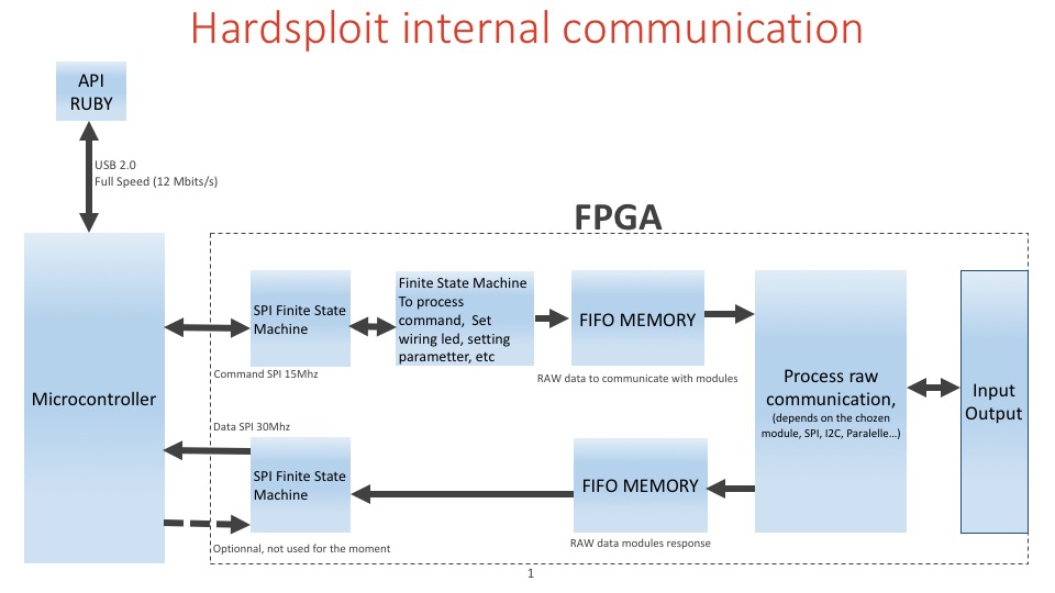
The parallel memory module for example, looks like the following. It will use the Core FPGA Hardsploit module.
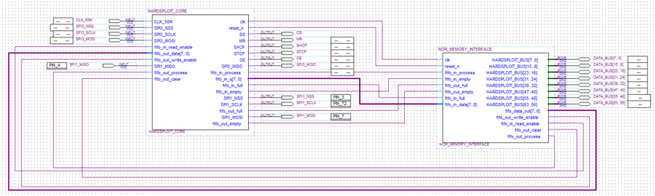
Harsploit core module is a bit complicated stuff
- One PLL to obtain 150Mhz from 50 Mhz oscillator.
- The core receive a command by SPI slave
- Set helping wiring functionality
- or fill the FIFO (First In First Out) memory to obtain a raw communication with each module (parallel memory, spi, I2C, 1Wire, etc)
- The module can send information to the second fifo and send the content to the microcontroller (uC) by spi master.
- There are 2 finite state machine to organize all tasks.
- Microcontroller send data to ruby for each receiving data by FPGA by DMA (Direct Access Memory) of the uC.
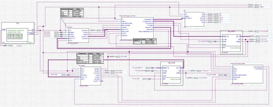
Simple? 🙂 Maybe a flowchart could help (or not ?)
In brief, we have created a FPGA module that is able to dump most of parallel memory chip. It will help security pentesters to dump firmware or all content contained in such memory in a easy way.
- Easier than if you need to create a dumping wiring function each time … No more arduino like board with plenty of wiring difficulties to connect to your chip, no more trouble to find the right memory command to be able to dump the component in front of you… The GUI will help you achieve that in few click only.
- Faster, as we use High Speed FPGA buses and machine state to achieved the dump.
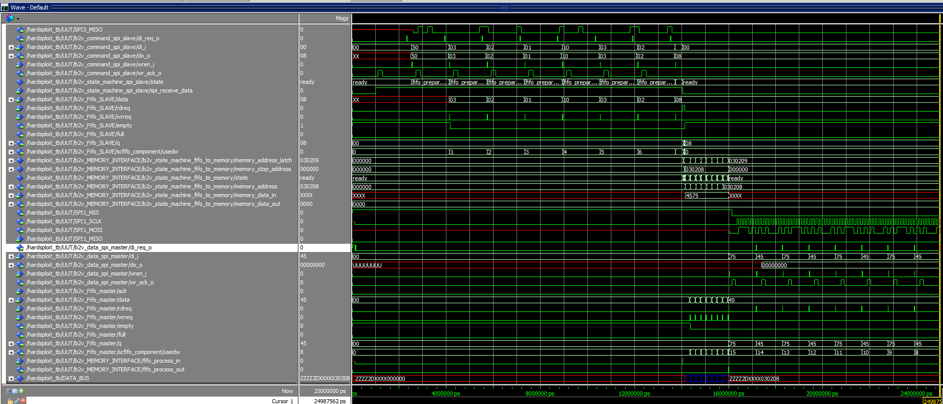
During our simulation and testing step, we succeed to dump parallel memory command with 3x8bits for address (see Graph Below)
What type of Memories we could dump for now?
- 32 bits for address / 8bits data = 4096 M => 4Go max
- 32 bits for address / 16bits data = 2×4096 M => 8Go max
Performance? Dumping Speed achieved (real world example – no bullshit)
For example, a dump of 128MByte memory chip.
- 1st result : only 5 to 10 min to read a embedded linux rom of 128MB.
More on dumping performance, according to our test ,
- Worst speed is 0.2MByte/s means less than 5 hour to read 4Go
- Average speed is 0.5MByte/s means about 2.2 hour for a dump of 4Go
- Max speed is 0.8MByte/s means about 80 min for a dump of 4Go
Just try to achieve that with other existing solution 😉
How to use that funky and (over) hype parallel dumping and writing function ?
We use our API (soon linked with the GUI…stay tuned)
We create a low level API with ruby that let you interact with FGPA module (Harsploit Module) in a simply way. See below an example of code we use. One function to call , few parameters to send (block to dump), few command to drive the chip. All those parameters will be soon pre input via the use of the GUI.
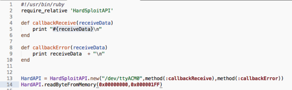 Simple as that !
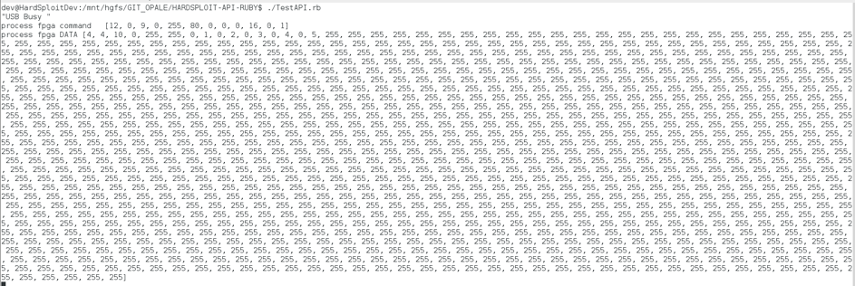
Results (with testing values – interesting data is at the beginning of the block)
Now you need to reverse the content of this memory and it’s your pentesters’ job 🙂
More information coming soon about several other Hardsploit Modules (I2C, SPI etc…)
Leave a Reply
You must be logged in to post a comment.